Feature creep, the project.
neon.Volt - so what is it?#
What is your favorite electronic gadget? I’m willing to put money on it being something like your phone or your iPad. If you think yourself clever, you might say an Arduino or something. As for me? It’s the power brick for my Steam Deck (followed closely by the Deck itself, I mean it’s basically a cyberdeck, but in contrast to the hobbyist ones you see, it’s actually good).
Why?#
I realized this after it became my go to charger for everything. It charges my phone, my tablet, my laptop. It runs my f*cking pinecil. As long as I had this in my bag, I felt safe.
As far as specs go, it’s perfectly average, which is ideal because that keeps it nice and compact. 45W, 20V 1.5A. It’s plenty for almost anything. Much like I mentioned in the intro for this project, I needed a portable, programmable source of power. So uh, let’s hack the power brick and make the 45 watts on that thing adjustable.
A switcher, not a negotiated passthrough?#
The folks at Pocket PD have a point. The power brick already has a buck converter inside. Why add another? All we need to do is to talk to the MCU running the show in there and that will get us all of the USB compliant voltages (5-20). In general, this is good enough for about 80% of the use cases for a device classified as an emergency replacement for a bench PSU. For my specific use case though? Well, I wanted to test motor control on it. That was the project I had in mind when I started this (and before everything spiralled). My specific BLDCs? System designed to run at 24V. Type C spec? Up to 20V. This is not the only reason though. The bulk of the remaining 20% that a programmable type C source will not cover is 3V3, which is essentially the be-all end-all of hobbyist logic rails. ESP32 - 3V3. Pico - 3V3. STM32F* - 3V3. Most of the general purpose MCUs are 5V tolerant, but they’re designed to run at 3V3 and making the PSU limited to just 5V is setting yourself up for issues down the line with stuff like ADC references and whatnot. The additional uses for the extended range include 1V8 and 1V1 logic, and on the top end, in addition to motor control, 24V, which is the main voltage for industrial automation and while I don’t really see anyone developing those systems on the neon.Volt, you can still technically do it. I know I will. On top of that, this opens up the potential use of the top range for testing the 24V systems’ overvoltage protections. For example.
So why a 4-switcher?#
The short answer is, because I like pain stumbled upon the IC by chance and I thought it’s really cool. I’ve never played with those before and I was aching for an excuse to do just that. And god knows I need to get better with I2C I was especially enamoured by the I2C control set on it.
So what is a 4-switcher? In short, it’s a DC-DC device that does both buck and boost (meaning it both reduces and increases voltage in relation to the input). It has all the parts for both of them and to complement that, it integrates an H-bridge gate driver. The specific part that I picked, LM51772, has 2 amps of drive strength so it can potentially drive some pretty beefy FETs. Before anyone says anything, I’m aware that there’s a version of this available that does the USB PD negotiation in addition to the boosting and the bucking, but I’ve been wanting to design around the STUSB4500 too, so this is a good opportunity. It enables some additional control that makes this build potentially more versatile, and the dedicated discharge paths on it fill me with confidence for both the safety and longevity of the end product.
System design#
On the top level, this project divides into 3 logical blocks: The input-output, power and control.
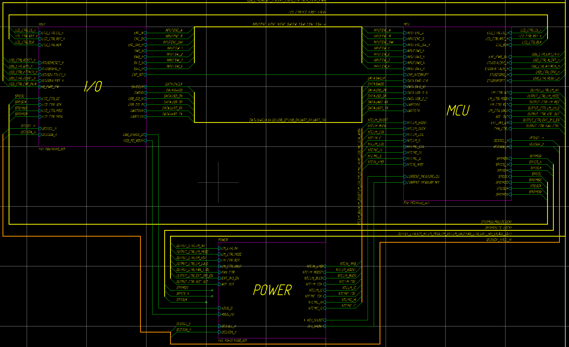
It’s quite hefty and this really pushes the bus handling capabilities of my sanity KiCAD. I’ve not really taken a deeper look into the software package as for the longest time, I’ve been obsessed with just finishing the schematics, but I’m aware that there should be a better way to work with buses across hierarchical sheets. Well, whatever. Let me break it down for you.
Power#
The main block of this design consists of 2 DC-DC nuggets and the main 4-switcher. First there’s a dedicated 3V3 rail for the control system, then there’s a separate, user accessible 3V3 rail - because honestly, you need this most of the time anyway and here you get a whole 1 amp of it. And this 1 amp is the sane version of what I originally had. I dialled it way back. The first iteration of this had an absolutely monstrous MIC2101 here. Something you might see in a VRM module on an ATX motherboard or a PSU - I mean, 12A for 3V3? What.
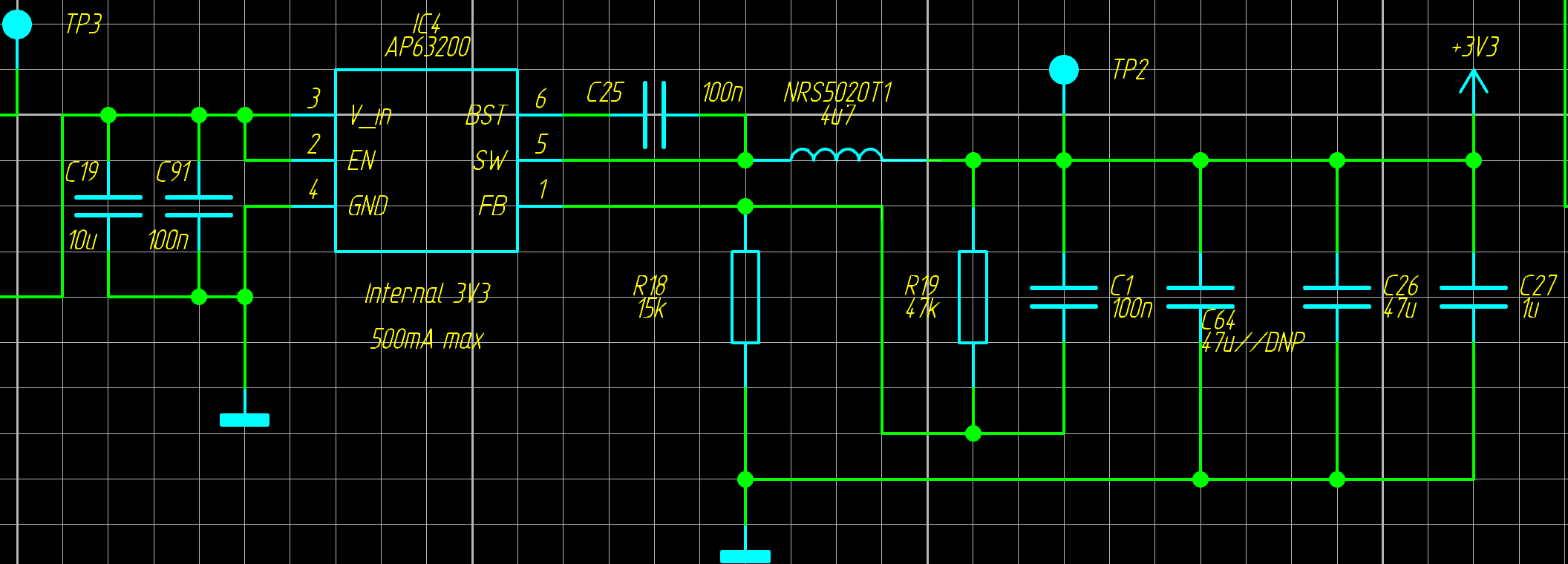
The 3V3 rails are both handled by the humble AP63200. It’s low cost and has a compact BOM. The FET is integrated. This means it needs some thermal consideration when doing layout, but in this application, it’s not too stressed. This is the 2A variant of the IC which means I can strangle it here a little. This is mostly on the account that only one of these rails is doing real current. That 1 amp of external power needs a bit of care, but the internal 3V3, I’ll be amazed if it ever crosses 100 mA of current. The only real power sink on this rail is the GPIO expander that can technically do 25mA per pin, but even loading this up 100% means I’m looking at 400mA + whatever the screen and MCU end up using. So on this board, it’s only operating at half and a quarter of the capacity, respectively. The only non-standard parts here are the test points, the rest is straight out of the datasheet.
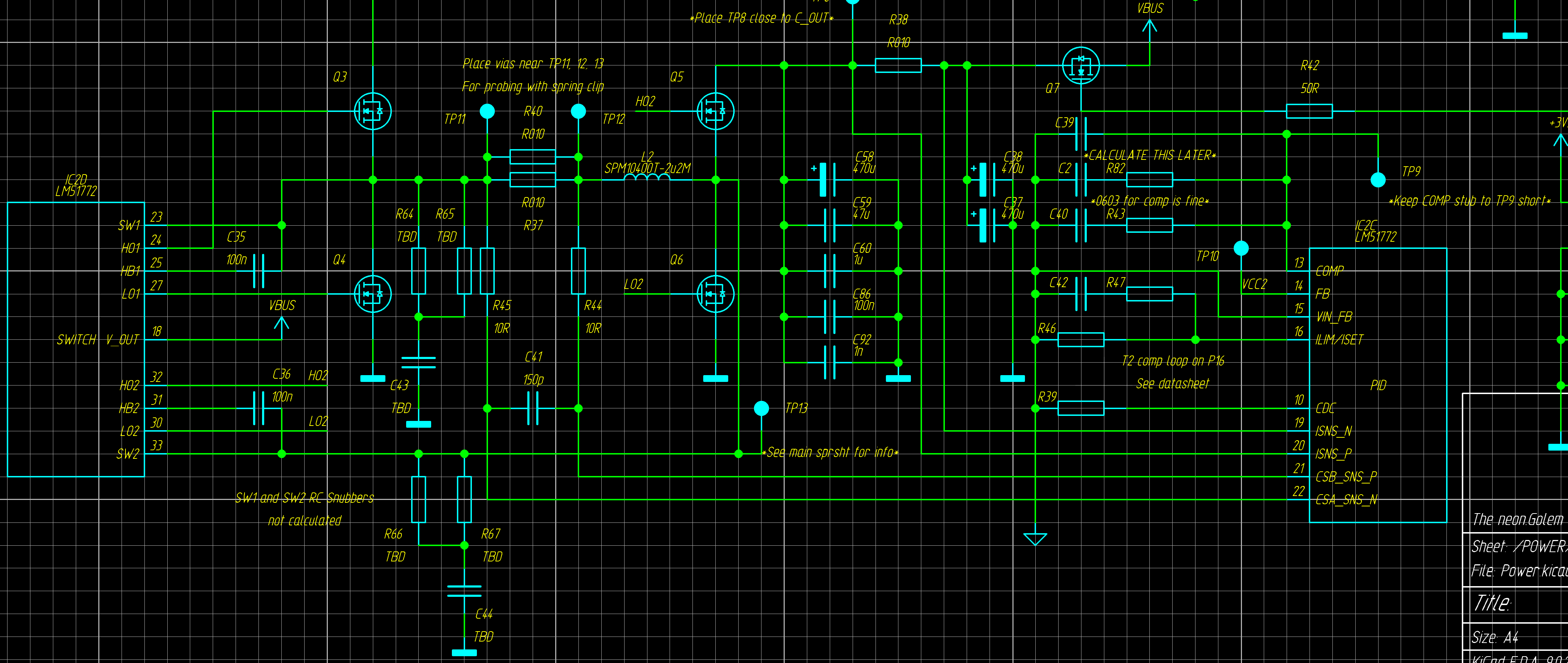
The LM51772 is what handles the adjustable rail. On paper, it is quite beautiful. up to 60V boost, as low as 1V buck and it can do that in 10mV steps (20mV past 20V - gotta double check this). My plan is to make this go from 1V to 30V, but I’m sizing the output TVS diodes to match that so that if I wanted, I could theoretically push it to its’ upper limit in terms of voltage. I’ve no idea what I’d even use 60V for to be honest. Off the top of my head, I only know one use case for this specific voltage - 12-14S LiPo. Or maybe solar stuff? But 48V is definitely of interest as that is the standard voltage for telecom. Then there’s stuff like extended industrial, DC BPL and low voltage EV/hybrid motors. Given the constraints of my input of 100W, this is probably not very useful, but simply having the option is better than nothing. It’s like when you don’t have a scope on hand, but you have a breadboard with a pico and some resistors on it. If you know roughly what you would be measuring, you can set up the ADC to sample this and log it over UART, then graph it in a spreadsheet. Is it good? No. But you’re no longer flying blind either. The current limits for the IC are eh, whatever - you pick. It doesn’t include the FETs so whatever you size your switching node to is what you can potentially push - so long as you lay it out right and respect the gate drive capability at your chosen frequency. Pushing past 5A continuous, on a PCB, takes careful deliberation. Control-wise, you have voltage and current control, overcurrent protection and a built in DRV pin to enable/disable the output. And it’s driven by I2C, so you save on GPIO. One of the better aspects of this chip is the efficiency at 20V input: 98.5%. You can clearly tell TI aimed this at USB PD. My schematic has a few non-standard parts here. The first thing you’ll notice is that there are RC snubbers on the switching node. Given the potential for a transient response of double digit amps per microsecond, this thing has the theoretical capability to mess up even your 3V3 logic that’s running nearby, to say nothing about 1V1 stuff, any kind of analog sensing or signal gen. I’ve also added test points here with ground vias close by to make measuring with a spring clip easier. The second non-standard thing is, I’m using a type 3 compensation loop here to push the performance a bit higher still. This is mainly because this device is meant to work at variable duty cycles so true optimization in the literal sense of the word is impossible. I can design for worst case and hope it doesn’t kill the performance in other, more lenient modes. It’s a current controlled switcher, too, so it doesn’t have the huge double pole at LC, which enables it to reach bandwidth numbers in the double digit kHz even with a poorly matched T2 comp loop, but with a T3 I can hopefully push it to somewhere around 60-80 kHz. The switching frequency on this guy is also controlled via I2C, which opens up potential for further optimization, but that’s a firmware thing, I won’t worry about that right now. Somewhere in a massive excel file I have the transfer function of this thing with the Bode plots for different values of compensation and the combined Bode plot for the whole loop, but I will go deeper into that in a future post.
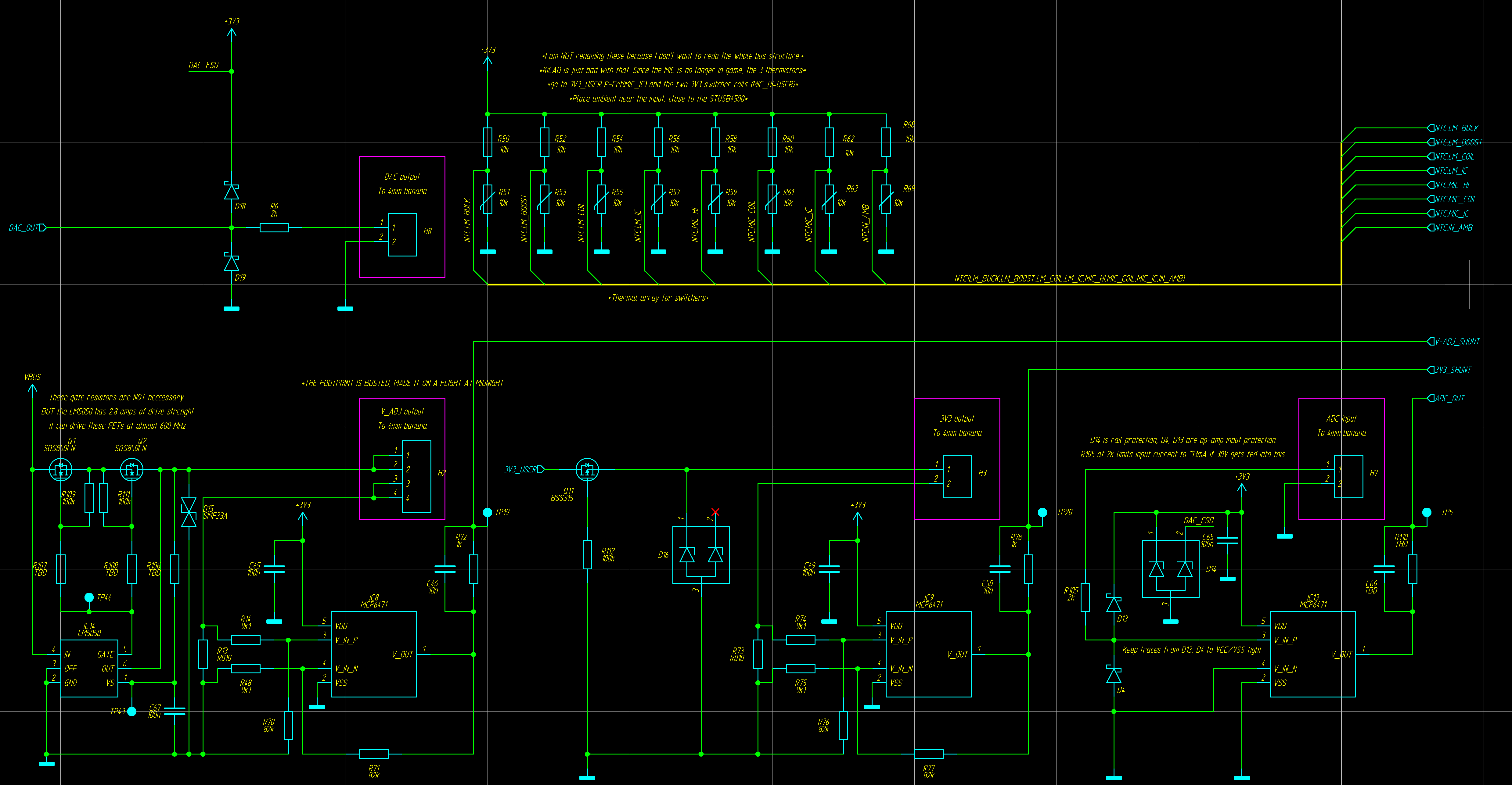
The final block here is the power output and thermal array. I have a thermistors on each of the major components. The KiCAD net labels are still from the initial design - I had too much of the bus structure already done and I wasn’t going to rename them just because I changed the structure a little. I’ll do it at a later date.
And then there’s some additional parts here that you wouldn’t expect to see on a power supply. This is where the feature creep comes in.
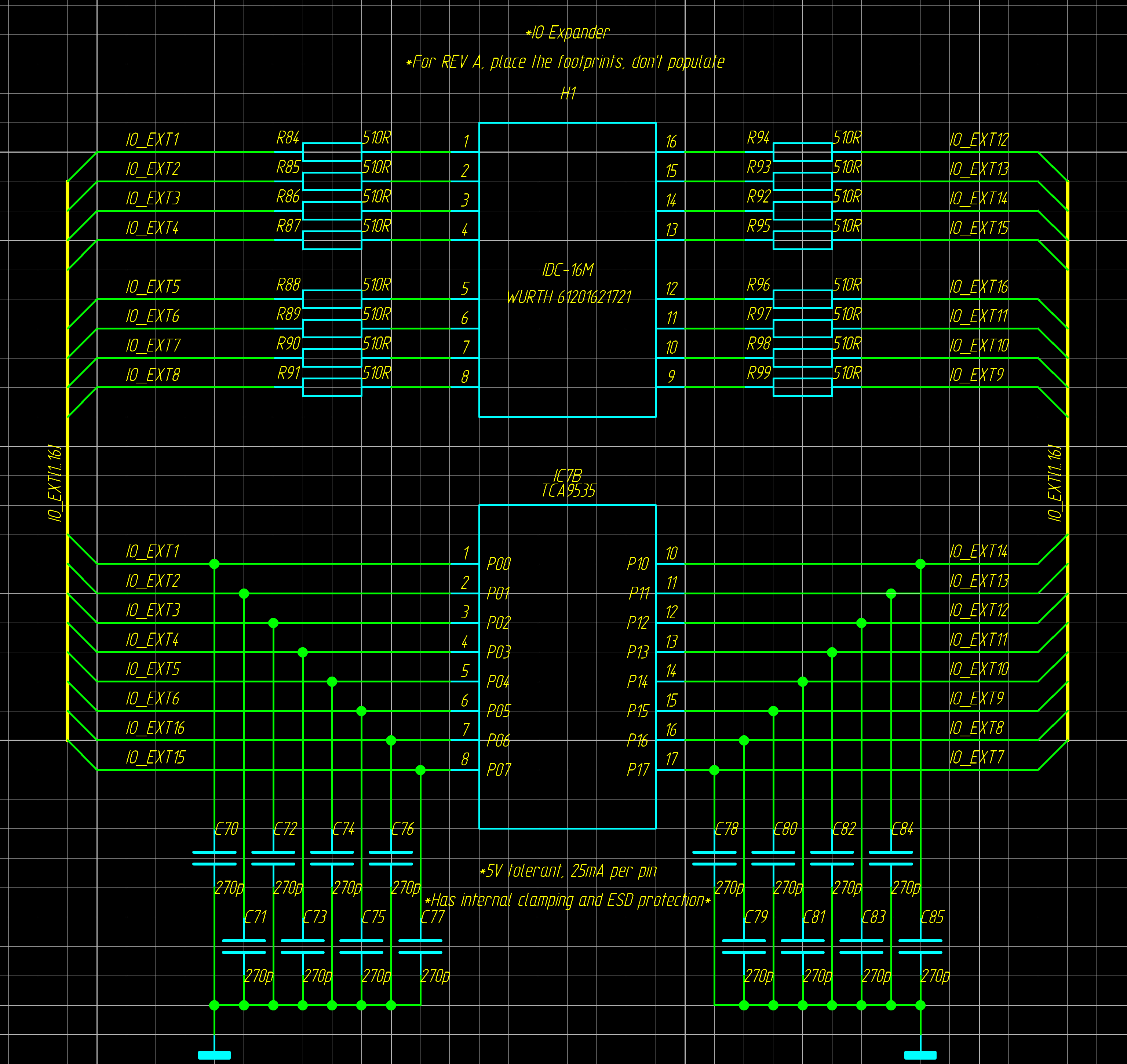
The idea here is basically, well you already have a 3V3 rail dedicated to your digital logic. What else would you want that you usually need but sometimes don’t have on hand? Some slow (400kHz) GPIO. And sure, I say it’s slow, but that’s in comparison to the brains of this machine, or any modern ARM MCU. It’s still plenty fast for many many things. And it’s actually not that much slower than something like an Arduino Uno.
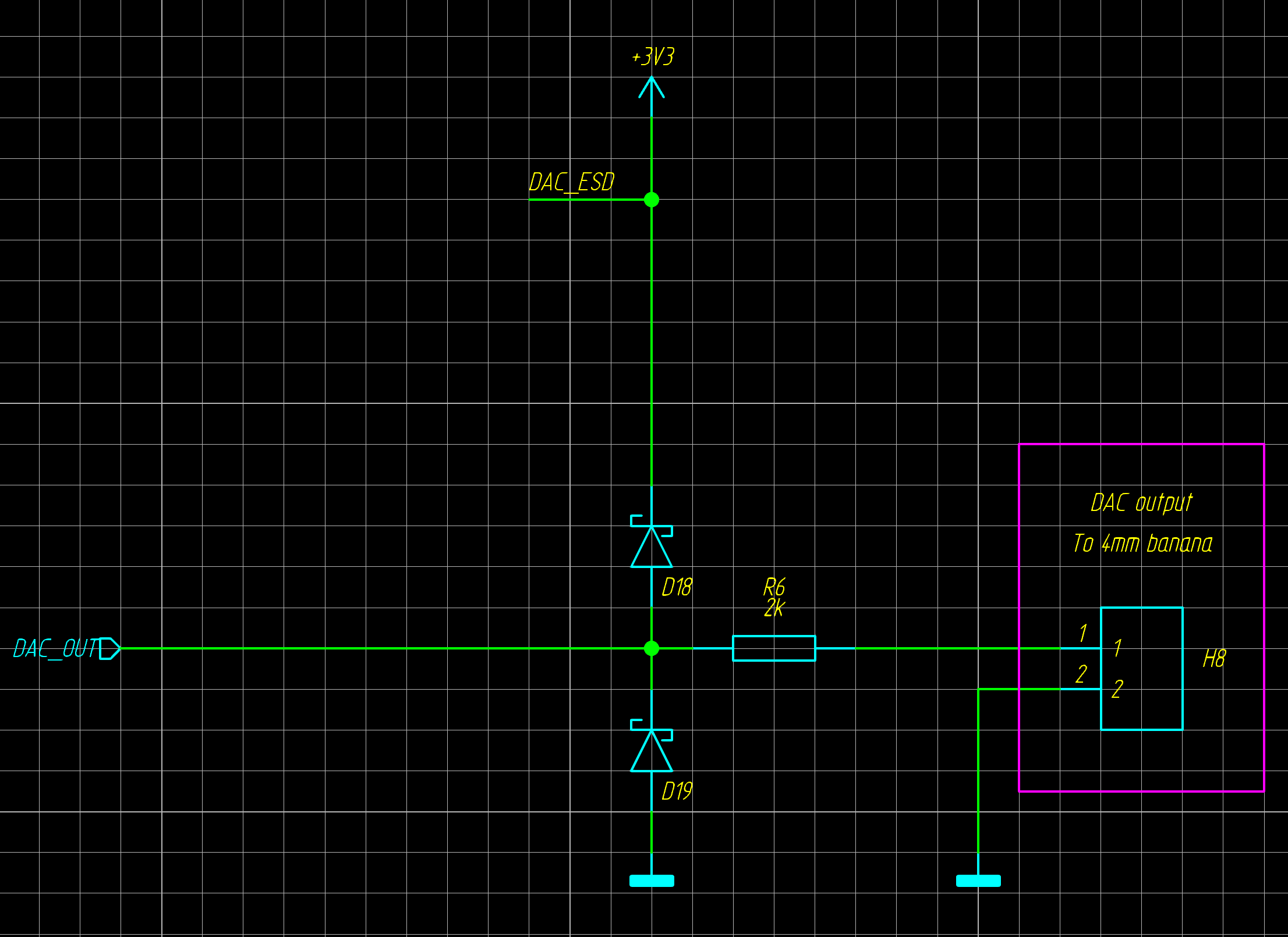
If GPIO is kind of sane then what the actual fuck is this? This is where I lost my mind a little. In hindsight, why is any of this here? The buffered ADC output (seen above), well, it’s here because there was an ADC pin free on the MCU. Simple as that. This isn’t even that feature-creepy, I mean it’s just an extra op-amp, one I already had on the BOM to boot. But why is there a DAC here? The observant will immediately have an answer - because of course it does. Adjustable voltage, adressable GPIO, addressable ADC - the only thing this portable lab multitool is missing is a signal generator. Now to be fair, I can’t push it too fast. It depends on SPI. I think I can push like 30 MHz on the RP2040 and the DAC itself should be fine with that too. Given the Nyquist theorem, restrictions of my RP2040 and some applied experience, I can maybe drive a decent sine out of this at 100kHz. Not great - but better than nothing. That said, I’m not sure I’ll ever even use it. I gave it a power rail that’s as solid as it can be. Maybe it’ll be useful. It’s an AD5621 - a 12 bit DAC from Analog. And I mean, I can’t afford power chips from Analog, but I wanted at least ONE IC from them on this. It’s like $4. Probably going to end up being like 10% of the BOM cost (of the PCBA). Odds are I won’t even populate the footprints, not on anything other than the first prototype. But the option is there.
I/O#
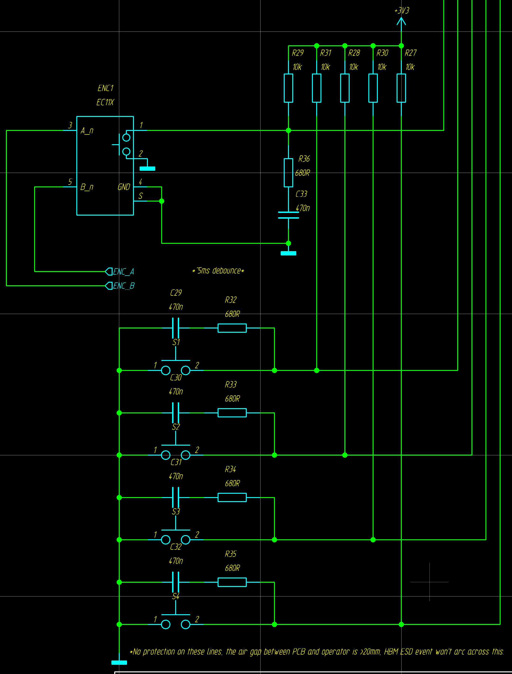
Okay so the inputs here are the bits I gave the least amount of thought to. I knew I wanted a rotary knob and I knew I wanted a good pushbutton experience - so I put CherryMX red switches here. It’s also got a regular old toggle switch for power (this just pulls the reset pin on the STUSB so it leaves the main power path closed, but leaves the digital logic powered). There’s an LCD here - an ILI9341 driven 2.8", 320x240 color screen with a transistor on the backlight pin (for adjustable brightness). the 320x240 was very deliberate - it’s very close to what Doom was originally ran at (320x200). Likewise for the CherryMX switches, like what else are you going to put on a gaming console? Well, a joystick or a more basic d-pad maybe, but that doesn’t sit right with me. On top of that, the screens are among the more “accessible” from AliExpress, they’re far better than the SSD1306/1309 OLEDs for resolution, similarly to those there’s an SPI driver available and they’re just flat out bigger. For a lab tool, this means it’s just easier to use.
Right. From the inputs you might actually find on a power supply, we have two USB Type C ports. Why two, you ask? Wait no, you’re not asking, you’re smart. You know that a data source will almost never push 100W of power. I know my laptop has fairly powerful type C ports, but I’ve never checked exactly what it puts out, but I doubt it’ll be pushing anything in the 20V range. Anyway, one is for debugging, programming and the eventual UART UI that I plan for this thing, the other is for power and they’re meant to be usable side by side with both plugged in.
Control#
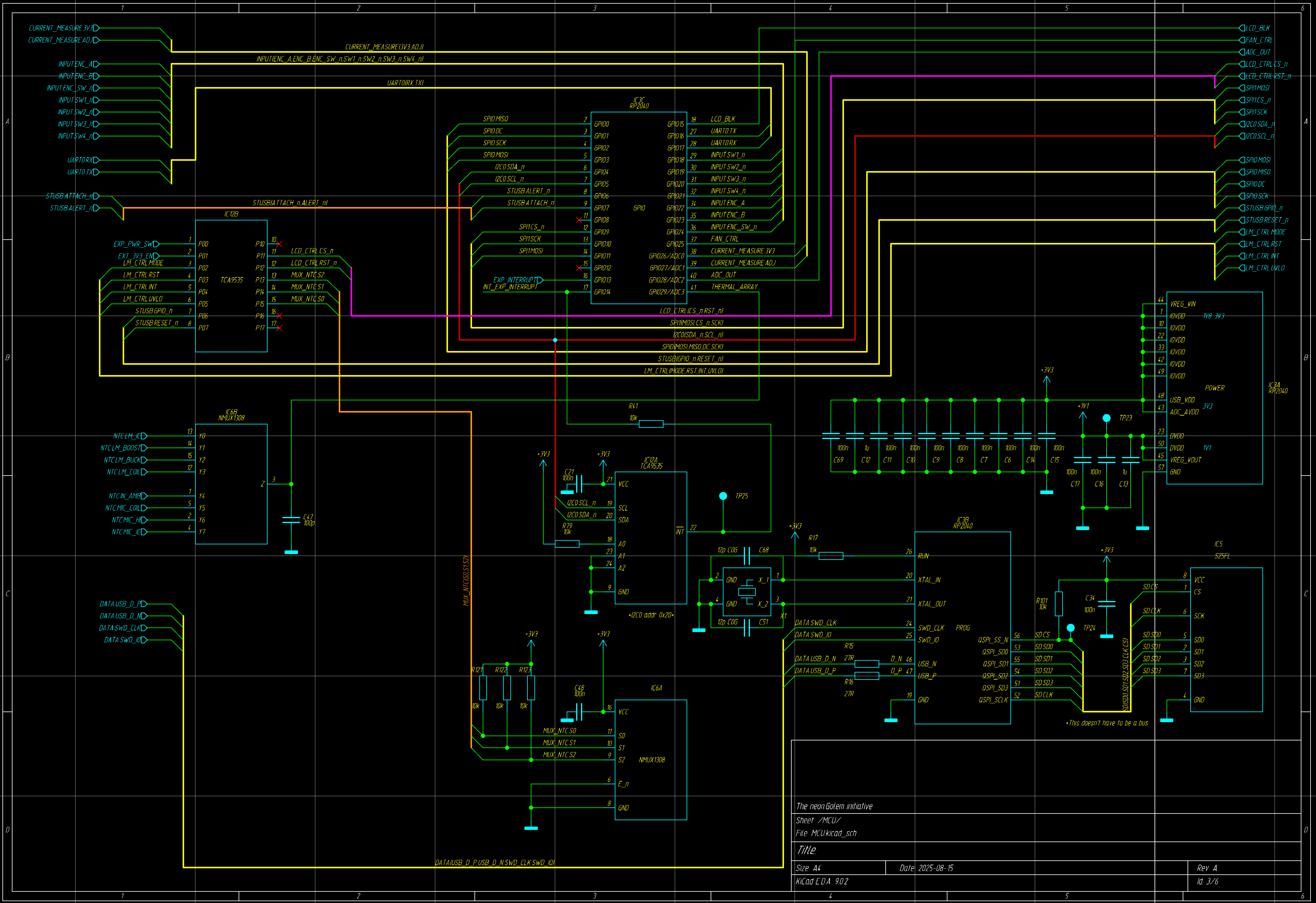
The MCU block is the one most resembling a spider web, but it’s not really that complicated. It’s got all the control signals, all the feedback signals, I2C and SPI. Since I don’t have enough pins on the MCU, I’ve enlisted the help of some multiplexers and an additional TCA9350 IO expander that has all the non-critical signals on it. I’m quite thankful that I can have the input switches and the encoder on dedicated GPIO, because this means these are all interrupt-enabled and that allows for some cool things, potentially. Some things I thought of adding as extra feature creep, but kept off the board because I’m not making a gaming console here they really made no sense: an IMU. A twin axis joystick.
That basically concludes the system design. This has taken me several months of work, going a few hours a week at most. Full schematics and the KiCAD project will be made public on my github soon-ish. Basically as soon as I verify that it actually works, I wouldn’t want to lead anyone into citing this as being true.
Firmware architecture coming up next. Given that we’re halfway through the fall semester, it might take me a while, but I want to document nuggets of information here and there. That means I should also post every now and then.